|
Properties of silicon and silicon wafers |
|
|
Properties of silicon and silicon wafers |
|
| Silicon material properties | Silicon wafer properties |
| 1. Crystal properties | 1. Properties |
| 2. Band structure properties | 2. Typical Sizes of Semiconductor Wafers |
| 3. Thermal properties | 3. Wafer Flats |
| 4. Electrical properties | 4. Cleaving |
| 5. Silicon etching | |
| 5. Mechanical properties |
|
PROPERTY |
VALUE |
UNITS |
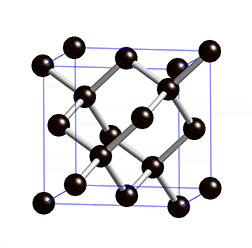
| Structure |
Cubic |
|
|
Space Group |
Fd3m |
|
|
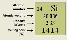
Atomic weight |
28.0855 |
|
|
Lattice spacing (a0 ) at 300K |
0.54311 |
nm |
|
Density at 300K |
2.3290 |
g/cm3 |
| Nearest Neighbour Distance at 300K | 0.235 | nm |
|
Number of atoms in 1 cm3 |
4.995 · 1022 |
|
|
Isotopes |
28 (92.23%) 29 ( 4.67%) 30 ( 3.10%) |
|
| Electron Shells |
1s22s22p63s23p2 |
|
| Common Ions | Si 4 +, Si 4 - | |
| Critical Pressure | 1450 | atm |
| Critical Temperature | 4920 | °C |
|
PROPERTY |
VALUE |
UNITS |
| Dielectric Constant at 300 K |
11.9 |
|
|
Effective density of states |
2.8x10¹⁹ |
cm-3 |
| Effective density of states (valence, Nv T=300 K ) |
1.04x10¹⁹ |
cm-3 |
| Electron affinity |
133.6 |
kJ / mol |
|
Energy Gap Eg at 300 K (Minimum Indirect Energy Gap at 300 K) |
1.12 |
eV |
|
Energy Gap Eg at ca. 0 K (Minimum Indirect Energy Gap at 0K) |
1.17 (at 0 K) |
eV |
| Minimum Direct Energy Gap at 300 K |
3.4 |
eV |
| Energy separation (EΓL) |
4.2 |
eV |
| Intrinsic Debye length |
24 |
um |
| Intrinsic carrier concentration |
1·1010 |
cm-3 |
| Intrinsic resistivity |
3.2·105 |
Ω·cm |
| Auger recombination coefficient Cn |
1.1·10-30 |
cm6 / s |
| Auger recombination coefficient Cp |
3·10-31 |
cm6 / s |
Temperature dependence of the energy gap:
Eg = 1.17 - 4.73·10-4·T2/(T+636) (eV)
where: T is temperature in degrees K.
|
PROPERTY |
VALUE |
UNITS |
|
Melting point |
1414 1687 |
°C K |
| Boiling point |
3538 |
K |
|
Specific heat |
0.7 |
J / (g x °C) |
|
Thermal conductivity [300K] |
148 |
W / (m x K) |
|
Thermal diffusivity |
0.8 |
cm2/s |
|
Thermal expansion, linear |
2.6·10-6 |
°C -1 |
|
Debye temperature |
640 |
K |
| Temperature dependence of band gap | -2.3e-4 | eV/K |
| Heat
of: fusion / vaporization / atomization |
39.6 / 383.3 / 452 |
kJ / mol |
|
PROPERTY |
VALUE |
UNITS |
|
Breakdown field |
≈ 3·105 |
V/cm |
| Index of refraction |
3.42 |
|
|
Mobility electrons |
≈ 1400 |
cm2 / (V x s) |
|
Mobility holes |
≈ 450 |
cm2 / (V x s) |
|
Diffusion coefficient electrons |
≈ 36 |
cm2/s |
|
Diffusion coefficient holes |
≈ 12 |
cm2/s |
|
Electron thermal velocity |
2.3·105 |
m/s |
| Electronegativity | 1.8 | Pauling`s |
|
Hole thermal velocity |
1.65·105 |
m/s |
|
Optical phonon energy |
0.063 |
eV |
| Density of surface atoms | (100)
6.78
(110) 9.59 (111) 7.83 |
1014/cm2
1014/cm2 1014/cm2 |
| Work function (intrinsic) | 4.15 | eV |
| Ionization Energies for Various Dopants |
Donors Sb 0.039 P 0.045 As 0.054 Acceptors
Al 0.067 Ga 0.072 In 0.16 |
eV eV eV
eV eV eV eV |
| PROPERTY | VALUE | UNITS | |
| Bulk modulus of elasticity | 9.8·1011 | dyn/cm2 | |
| Density | 2.329 | g/cm3 | |
| Hardness | 7 | on the Mohs scale | |
| Surface microhardness (using Knoop's pyramid test) | 1150 | kg/mm2 | |
| Elastic constants |
C11 = 16.60·1011
C12 = 6.40·1011 C44 = 7.96·1011 |
dyn/cm2
dyn/cm2 dyn/cm2 |
|
| Young's Modulus (E) | [100] [110][111] |
129.5 168.0 186.5 |
GPa GPa GPa |
| Shear Modulus | 64.1 | GPa | |
| Poisson's Ratio | 0.22 to 0.28 | - | |
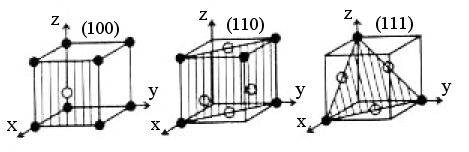
Silicon wafers propertiesSilicon, Si - the most common semiconductor, single crystal Si can be processed into wafers up to 300 mm in diameter. Wafers are thin (thickness depends on wafer diameter, but is typically less than 1 mm), circular slice of single-crystal semiconductor material cut from the ingot of single crystal semiconductor. All lattice planes and lattice directions are described by a mathematical description known as a Miller Index. In the cubic lattice system, the direction [hkl] defines a vector direction normal to surface of a particular plane or facet. A crystal can always be divided into a fundamental shape with a characteristic shape, volume, and contents.
As a crystal is periodic, there exist families of equivalent directions and planes. Notation allows for distinction between a specific direction or plane and families of such. Miller convention:
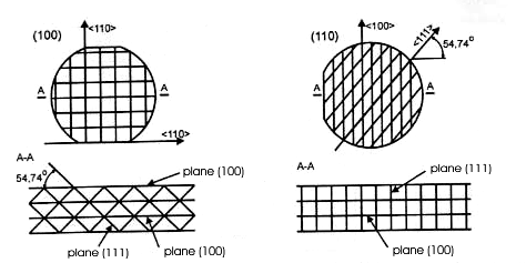
Planes configurations for (100) and (110) wafers:
Angles Between Planes
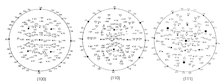
Stereographic projection of silicon crystal:
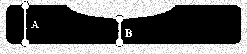
TTV = A -
B
GTIR = A +
B
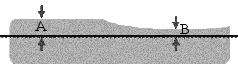
An n-type (negative-type) extrinsic silicon semiconductor is a semiconducting material that was produced by doping silicon with an n-type element of Group V A, such as P, As, or Sb. Consequently, electrons are the majority charge carriers of the material. A p-type (positive-type) extrinsic silicon semiconductor is a semiconducting material that was produced by doping silicon with an p-type element of group III A, such as B, Al, or Ga. Since the dopants are acceptor atoms, holes are the majority charge carriers of the material. Measurement of wafer characteristics - dark field and bright field detection
1. Typical Sizes of Semicoductor Wafers(The Diameter of a wafer is measured through its center and not through any flats): 1 inch or 25mm
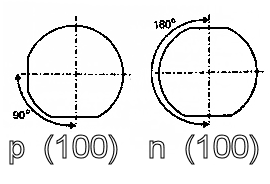
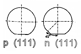
2. Wafer Flats - orientation for automatic equipment and indicate type and orientation of crystal.Primary flat – The flat of longest length located in the circumference of the wafer. The primary flat has a specific crystal orientation relative to the wafer surface; major flat. Secondary flat – Indicates the crystal orientation and doping of the wafer.
3. CleavingCleaves will run according to the crystal orientations. If the crystal orientation of the Si is <100> cleave at 90 deg. angles.
If the crystal orientation of the Si is <111> cleave at 60 deg. angles.
5. Silicon etchingIn general, there are two classes of etching processes:
Wet etchingWet etching is a blanket name that covers the removal of material by immersing the wafer in a liquid bath of the chemical etchant. Wet etchants fall into two broad categories; isotropic etchants and anisotropic etchants.
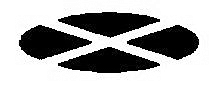
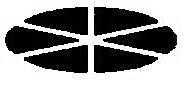
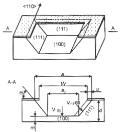
Silicon, exhibit anisotropic etching in certain chemicals. Anisotropic etching in contrast to isotropic etching means different etch rates in different directions in the material. The classic example of this is the <111> crystal plane sidewalls that appear when etching a hole in a <100> silicon wafer in a chemical such as potassium hydroxide (KOH). The result is a pyramid shaped hole instead of a hole with rounded sidewalls with a isotropic etchant.
Plane hkl etching speed: Vhkl =dhkl / t where: dhkl - etching deep, t - etching time
EXAMPLE: Silicon membrane
|
||||||||||||||||||||||||||||||||||||||||||||||||||||
Dry etchingThe most common form of dry etching is reactive ion etching (RIE). Ions are accelerated towards the material to be etched, and the etching reaction is enhanced in the direction of travel of the ion. RIE is an anisotropic etching technique. RIE is not limited by the crystal planes in the silicon.
Web Site Developed By: Lukasz Sikora |
||||||||||||||||||||||||||||||||||||||||||||||||||||